
Scientists have created the thinnest optical lens ever made for camera systems. At just three atoms thick, the researchers believe it will be especially useful for future wearables like the now defunct Google Glass or Meta’s RayBan smart glasses.
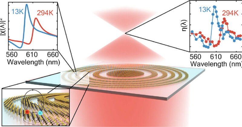
This flat lens, which was published to the Nano Letters journal, otherwise known as a metalens or metasurface, is absurdly thin: 0.0000006 millimeters, or 0.6 nanometers, thick; the height of three atoms. As explained by Phys, the researchers from the University of Amsterdam and Stanford University used a different technique to develop this lens compared to traditional optics.
Typically, curved glass is used to bend and refract light when it enters an array and again when it exits, making objects appear closer than they are. But in recent years, scientists have experimented with meta surfaces as a replacement for these traditional glass optics to address the main issue with them: they tend to be quite large. Right now, camera makers are restricted by physics: multiple glass elements take up space and in smartphones and on wearables, space is at a premium.
Metalenses are flat surfaces that are designed to replace full-size optics with a wholly different method. Instead of curved optics, they reduce the aforementioned multiple glass optical systems by compressing them into a much smaller system that bends light using nanoparticles and metasurfaces.
These types of flat lenses have not made it into consumer imaging products yet but researchers continue to push the boundaries of what is possible with the concept. In this case, the researchers used a unique material called tungsten disulfide. Instead of a curved glass lens, this metalens uses concentric rings of tungsten disulfide with gaps in between, which is the same concept that is used with Fresnel lenses — they focus light using diffraction instead of refraction.
The focusing efficiency of this super-thin lens relies on quantum effects within tungsten disulfide, allowing the material to absorb and re-emit light at specific wavelengths, Phys explains.
The scientists are especially excited about another unique feature of this metalens: when light passes through it, it makes a bright focal point and most of the light is unaffected. That may sound like a disadvantage, but there is a way to take advantage of this.
“The lens can be used in applications where the view through the lens should not be disturbed, but a small part of the light can be tapped to collect information. This makes it perfect for wearable glasses such as for augmented reality,” explains Jorik van de Groep, one of the researchers and authors of the paper.
As mentioned, metalenses aren’t yet to the operational capability to see them installed on consumer devices, but multiple companies are working in the field including a company entirely devoted to it, Metalenz, and Canon. The technology isn’t quite there yet, but developments are happening rapidly and it’s only a matter of time.
Image credits: ‘Temperature-Dependent Excitonic Light Manipulation with Atomically Thin Optical Elements’ by Guarneri, Li, Bauer, Song, Saunders, Liu, Brongersma, and van de Groep.